M28F101 Datasheet – 1Mb 128Kx8, Chip Erase Flash Memory IC
By Hamza Khan

Overview
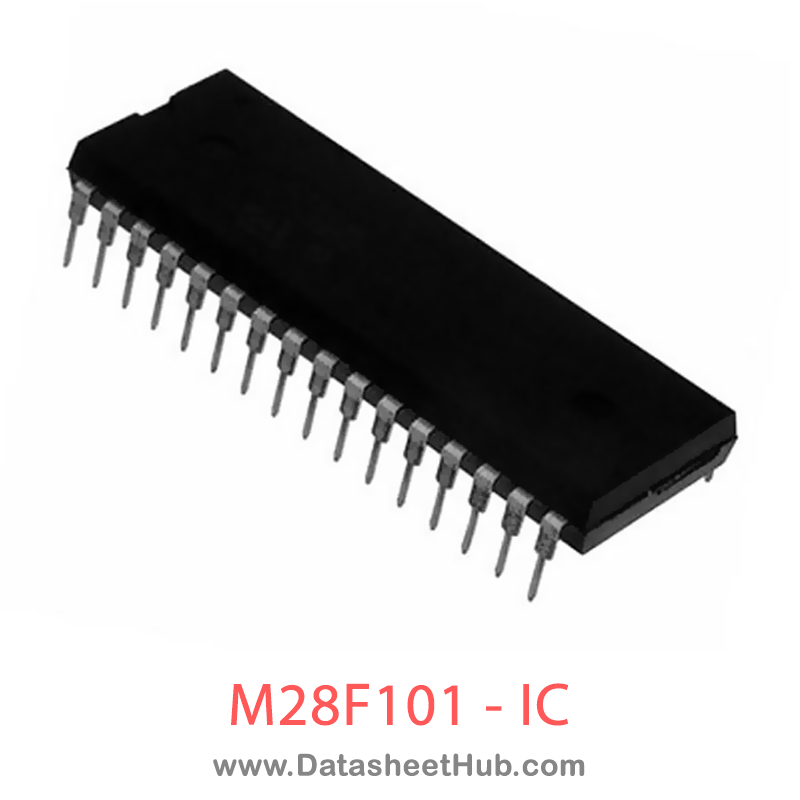
The M28F101 FLASH Memory is a non-volatile memory that may be erased electrically at the chip level and programmed byte-by-byte. It is or- gained as 128K bytes of 8 bits. It uses a command register architecture to select the operating modes and thus provides a simple microprocessor inter- face. The M28F101 FLASH Memory is suitable for applications where the memory has to be reprogrammed in the equipment. The access time of 70ns makes the device suitable for use in high-speed microprocessor systems.
| Part Number | M28F101 |
| Function | 1 Mb (128K x 8, Chip Erase) FLASH MEMORY |
| Package | DIP, PLCC, TSOP 32 Pin Type |
| Manufacturer | STMicroelectronics |
| Datasheet | Download PDF  |
M28F101 Features
- 5V±10% SUPPLY VOLTAGE
- 12V PROGRAMMING VOLTAGE
- FAST ACCESS TIME: 70ns
- BYTE PROGRAMMING TIME: 10µs typical
- ELECTRICAL CHIP ERASE in 1s RANGE
- LOW POWER CONSUMPTION – Stand-by Current: 100µA max
- 10,000 ERASE/PROGRAM CYCLES
- INTEGRATED ERASE/PROGRAM-STOP TIMER
- OTP COMPATIBLE PACKAGES and PINOUTS
- ELECTRONIC SIGNATURE
- Manufacturer Code: 20h
- Device Code: 07h
Absolute Maximum Ratings
| Symbol | Parameter | Value | Unit |
| TA | Ambient Operating Temperature | –40 to 125 | °C |
| TSTG | Storage Temperature | –65 to 150 | °C |
| VIO | Input or Output Voltages | –0.6 to 7 | V |
| VCC | Supply Voltage | –0.6 to 7 | V |
| VA9 | A9 Voltage | –0.6 to 13.5 | V |
| Vpp | Program Supply Voltage, during Erase or Programming | –0.6 to 14 | V |
M28F101 Pinout
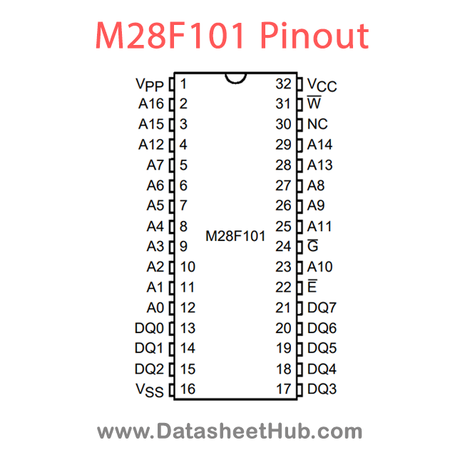
Pin Definitions
| Pin Name | Description |
|---|---|
| A0-A16 | Address Inputs |
| DQ0-DQ7 | Data Inputs / Outputs |
| E | Chip Enable |
| G | Output Enable |
| W | Write Enable |
| VPP | Program Supply |
| VCC | Supply Voltage |
| VSS | Ground |
Applications
- Non-volatile storage
- Embedded systems
- Firmware storage
- Program code storage
- Bootloader memory
M28F101 Datasheet
Download the M28F101 IC Datasheet from the link given below.
Comments 0
Leave a comment